
Here is the conclusion first: the most “invisible” bottleneck in semiconductor equipment may not be the lithography machine, but the unassuming vacuum valve sitting inside the vacuum chamber — about 90% of advanced-process vacuum valves globally are still imported, and China’s localization rate is under 2%.
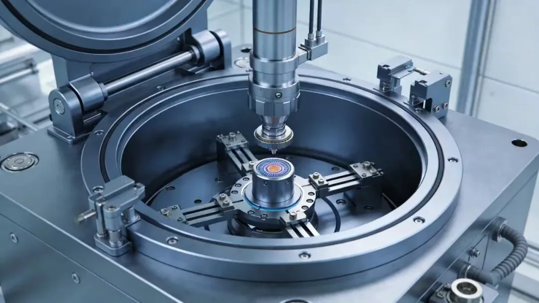
What Delays Etchers Is Not the Litho Machine
Ask people about semiconductor “bottlenecks” and they first think of the lithography machine. But what really pushes a line of domestic equipment makers to keep extending delivery times downstream is often a far humbler part — the vacuum valve. The numbers are stark: Switzerland’s VAT alone takes about 70% of the global semiconductor vacuum-valve market, and over 90% in advanced processes. Domestic vacuum valves: overall localization under 15%, and under 2% in advanced processes (including HBM) (source: Semiconductor Industry Observer, 2026). In other words, the hardest thing to crack may not be the “exposure machine” but the small valve that opens and closes, isolates and seals the chamber.
Why a Single Valve Can Bottleneck a Production Line
Etching, thin-film deposition and ion implantation — all three “dry-process” tools must run inside a tightly controlled vacuum chamber: process gas comes in, by-products are pumped out, and the chamber is repeatedly isolated — all relying on a system of vacuum valves and valve parts to “close the door and open it”. Three requirements: ultra-high vacuum — leak rates checked below the 10¹¹? order; ultra-clean — any metal ions released or particles shed by the valve body and seals directly contaminate the wafer; and corrosion resistance — under aggressive process gas, the material must both withstand corrosion and keep its dimensions from drifting. In one sentence: the vacuum valve decides the delivery cadence of the three core tool types, twice the “least conspicuous yet most critical” link in the equipment chain (per National Semiconductor Industry Alliance, 2026).
This Hollow Is Deeper Than the Tool-Localization Number
There is a comparison often missed: overall semiconductor tool localization was about 30% in 2025 and is expected to reach 42% by 2027 — the curve is climbing. But split the progress bar and vacuum components are the deepest hollow, dragging the whole chain’s cadence. The urgency is real: under the geographic situation, imported vacuum-component lead times lengthen and prices rise, while domestic lines and replacements happen at the same time, releasing demand in a concentrated wave. The substitution window is open — but it will not stay open. At this point the contest is not price but delivery stability and consistency: once a customer validates a supplier and pulls them into stable supply, replacement becomes extremely hard. Whoever gets the “entry ticket” first locks into the supply chain.
The “Invisible Material War” Inside the Chamber
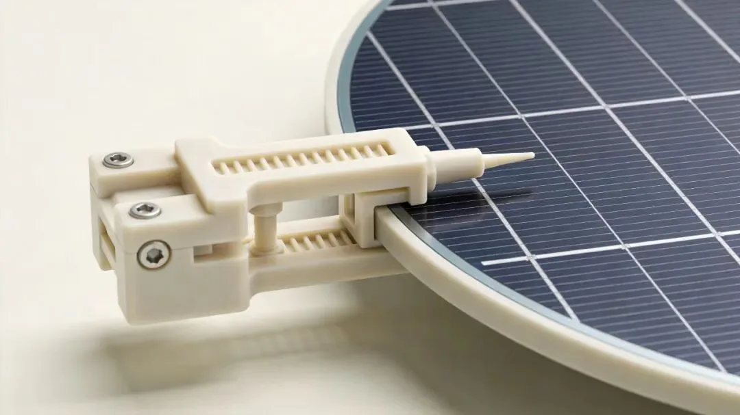
The valve itself is a precise combination of metal and seals. But look across the whole vacuum/clean room chamber and there is another often-overlooked corner: insulation parts, locating bushings, wafer-transport and gripping parts, and vacuum-seal support parts. These parts must not conduct, must not release metal ions, must not shed particles, and must still resist high temperature and corrosion. Metal parts carry ion-release and debris risks, while ordinary plastics cannot survive high-temperature process gas — which is why PEEK (polyether ether ketone) is repeatedly named: ultra-clean and low-outgassing, heat-resistant to 260°C, wear-resistant with low particles, and insulating with an adjustable conductive grade. For this reason, the grippers and suction nozzles of wafer-transport systems, the fixing supports and flow-guide components of wet-cleaning baths, precision locating bushings, insulation isolators, micro transmission parts, and vacuum-seal support parts are all often made of PEEK.
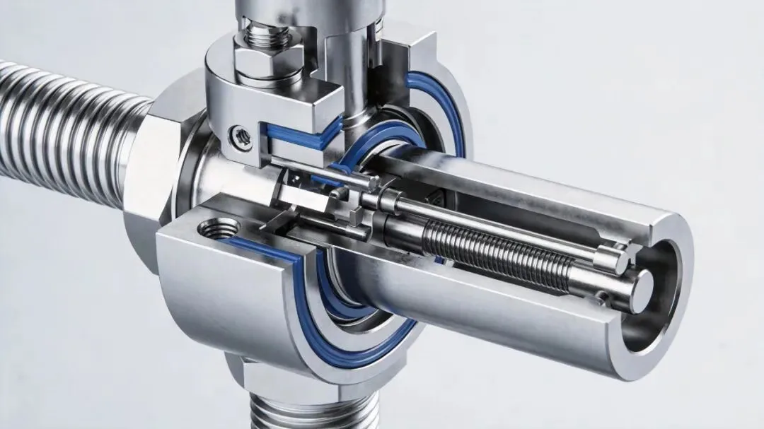
An honest boundary: under long-duration strong plasma bombardment, PEEK does also experience etch loss, so a life assessment must weigh temperature, media, plasma environment and mechanical load together — it cannot be applied one-size-fits-all.
From “90% Imported” to a “Material Breakthrough”
Zoom out from the materials-selection logic and this localization is, at its core, a consistency engineering project “from material to part”. Upstream, high-purity monomers make PEEK resin’s cleanliness, temperature resistance and wear resistance solid. Midstream, modified formulations tune stiffness, wear and static behavior to each station’s need. Downstream, precision molding machines wafer clamps, bushings and insulation seats to runout of 0.01 mm and surface roughness of Ra0.4 micron. Only when all three links are stable can domestic PEEK structural parts in the vacuum chamber truly replace imported ones and hold yield. This is exactly the path specialty engineering plastics has long worked — the PEEK modified materials and precision injection molding Dalian Luyang Technology is engaged in sit exactly on this “one line from material to part”, supporting these high-cleanliness, high-wear, high-dimensional-stability structural parts.
The Right Posture for the Window: Secure Delivery First, Then Performance
Substitution, in the short term, is about delivery stability, not a single performance metric. Between the tool localization rate climbing from 30% toward 42%, whether the “small parts” — vacuum valves, vacuum pumps, seals and insulation parts — can supply stably and batch-consistently decides whether downstream dares to loosen adoption. Domestic dry vacuum-pump maker Zhongkeyi has shipped more than 40,000 units cumulatively, over 30,000 into integrated circuits, proving the “validate – adopt – scale” road (source: Zhongkeyi public disclosure, 2026). In the vacuum-valve field, domestic makers have already replaced about 15% at some nodes, with advanced processes still the hardest bone to chew.
What Stays at This Threshold Is “Daring to Switch” and “Knowing How to Switch”
Back to the valve at the start: over 90% of advanced-process vacuum valves are imported — that is a fact, but the number is not static. Tool localization is speeding up, expansion and replacement are concentrating, the geographic situation keeps adding uncertainty — this substitution window is open right now; and substitution is not a one-shot deal, it is whether the whole chain can hold up: from the “hardware” of the vacuum valve, to the “tough structural parts” of PEEK insulation parts, bushings and carriers inside the chamber, to material modification and precision molding. For the material side, whoever makes high-cleanliness, high-wear, high-dimensional-stability PEEK modified materials and precision-molded parts into a reliable supply stands at the starting line of this localization wave. From Dalian Luyang Technology, a specialty-engineering-plastics manufacturer working in PEEK, PI and PTFE modification and precision injection molding for high-cleanliness wafer carriers, locating bushings, insulation isolators and vacuum-seal support parts in semiconductor equipment.